Tensor Processing Units
Sumit Yadav (PUL076BCT088)
Director, Information Technology Innovation Center, Tribhuvan University
Computer Organization and Architecture — 09 June 2022
Full paper PDF: TPUs-2.pdf
TPUs (Tensor Processing Unit)
Tensor Processing Units (TPUs) are custom-designed application-specific integrated circuits (ASICs) developed by Google to accelerate AI and neural network workloads. Formally, development began in 2015 and TPUs were first made publicly available in 2018 for both cloud computing and small businesses. The TPU was first introduced at Google I/O in 2016, when Google revealed that the chip had already been used internally for over a year.
This chip is specific to machine learning frameworks like TensorFlow, PyTorch, and JAX. A TPU is another kind of processing unit — like a CPU or a GPU — but with important differences. The biggest is that a TPU is an ASIC: unlike CPUs and GPUs, it is optimised to do one specific class of application.
CPU, GPU and TPU
Let's compare the three processors for the case of a matrix multiply-add operation:
- A CPU performs multiply-add by reading each input and weight from memory, multiplying them with its ALU (Arithmetic Logic Unit), writing results back to memory, and finally summing the products. Modern CPUs compensate with massive caches, branch prediction, and high clock rates — all of which contribute to lower latency.
- A GPU forgoes those latency-reducing features and instead orchestrates thousands of ALUs in parallel. GPUs dramatically increase throughput by parallelising computation, at the cost of higher latency per operation.
- A TPU operates very differently: its ALUs are directly connected to each other without going through memory. Data is passed directly between ALUs, which drastically reduces latency.
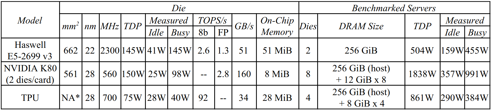
Table 1. Benchmarked servers use Haswell CPUs, K80 GPUs, and TPUs. Haswell has 18 cores; the K80 has 13 SMX processors.
Workload guidance (when training AI models):
CPUs are best for:
- Quick prototyping requiring maximum flexibility
- Simple models that do not take long to train
- Models dominated by custom TensorFlow operations written in C++
- Models limited by available I/O or host machine networking bandwidth
GPUs are best for:
- Models whose source does not exist or is too onerous to change
- Models with a significant number of custom TensorFlow operations that must run at least partially on CPUs
- Models with TensorFlow ops not available on Cloud TPU
- Medium-to-large models with larger effective batch sizes
TPUs are best for:
- Models dominated by matrix computation
- Models with no custom TensorFlow operations inside the main training loop
- Models that train for weeks or months
- Larger and very large models with very large effective batch sizes
TPU Origin, Architecture, and Implementation
Starting as early as 2006, Google discussed deploying GPUs, FPGAs, or custom ASICs in its datacenters. The conclusion was that the few applications that could run on special hardware could be handled virtually for free using excess datacenter capacity — and it is hard to improve on free. The conversation changed in 2013 when a projection showed that if people used voice search for three minutes a day with speech-recognition DNNs, datacenter capacity would need to double, which would be very expensive using conventional CPUs. Google therefore started a high-priority project to quickly produce a custom ASIC for inference (and bought off-the-shelf GPUs for training). The goal was to improve cost-performance by 10× over GPUs. Given this mandate, the TPU was designed, verified, built, and deployed in datacenters in just 15 months.
Rather than being tightly integrated with a CPU — which would risk delaying deployment — the TPU was designed as a coprocessor on the PCIe I/O bus, allowing it to plug into existing servers just as a GPU does. To simplify hardware design and debugging, the host server sends TPU instructions for it to execute rather than the TPU fetching them itself. In spirit, the TPU is closer to an FPU coprocessor than to a GPU.
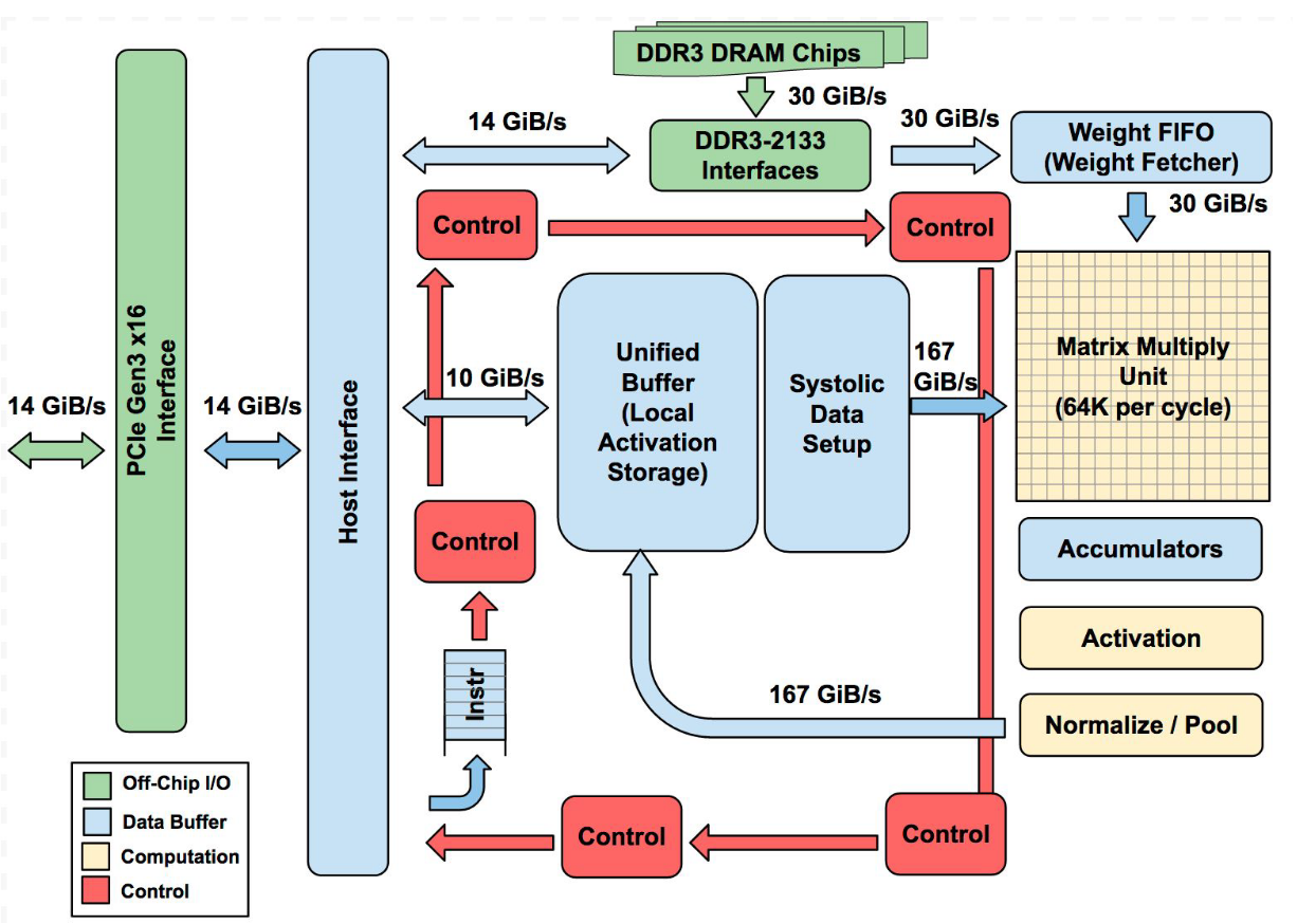
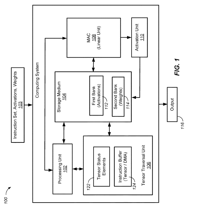
Fig 1. TPU Block Diagram. The main computation part is the yellow Matrix Multiply unit (upper right). Its inputs are the blue Weight FIFO and the blue Unified Buffer (UB); its output feeds the blue Accumulators (Acc). The yellow Activation Unit performs nonlinear functions on the Acc and writes results to the UB.
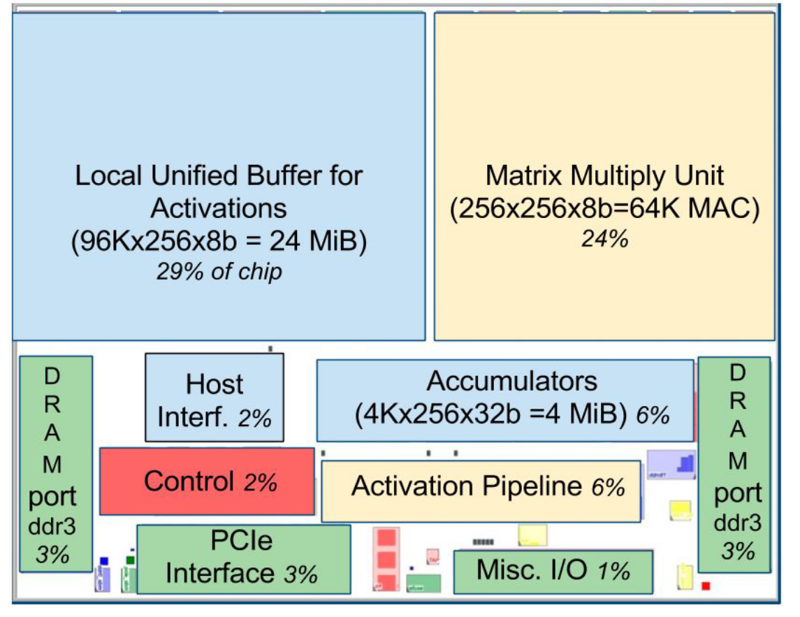
Fig 2. Floor Plan of TPU die. Light (blue) data buffers are 37% of the die, light (yellow) compute is 30%, medium (green) I/O is 10%, and dark (red) control is just 2%. Control is much larger (and much more difficult to design) in a CPU or GPU.
The goal was to run whole inference models in the TPU — to reduce interactions with the host CPU — and to be flexible enough to match NN needs beyond 2015. Figure 1 shows the block diagram.
TPU instructions are sent from the host over the PCIe Gen3 x16 bus into an instruction buffer. Internal blocks are typically connected by 256-byte-wide paths. Starting in the upper-right corner, the Matrix Multiply Unit is the heart of the TPU. It contains 256×256 MACs that can perform 8-bit multiply-and-adds on signed or unsigned integers. The 16-bit products are collected in 4 MiB of 32-bit Accumulators below the matrix unit — specifically 4096 256-element 32-bit accumulators. The matrix unit produces one 256-element partial sum per clock cycle.
When using a mix of 8-bit weights and 16-bit activations (or vice versa), the Matrix Unit runs at half-speed; when both are 16-bit it runs at quarter-speed. It reads and writes 256 values per clock cycle and can perform either matrix multiply or convolution. The matrix unit holds one 64 KiB tile of weights plus one for double-buffering (to hide the 256 cycles required to shift a tile in). This unit is designed for dense matrices — sparse architectural support was omitted for time-to-deploy reasons.
Weights are staged through an on-chip Weight FIFO that reads from an off-chip 8 GiB DRAM called Weight Memory (weights are read-only during inference; 8 GiB supports many simultaneously active models). The Weight FIFO is four tiles deep. Intermediate results are held in the 24 MiB on-chip Unified Buffer, which serves as input to the Matrix Unit. A programmable DMA controller transfers data to/from CPU host memory and the Unified Buffer.
As instructions are sent over the relatively slow PCIe bus, TPU instructions follow the CISC tradition, including a repeat field. The average CPI is typically 10 to 20. There are about a dozen instructions; the five key ones are:
- Read_Host_Memory — reads data from CPU host memory into the Unified Buffer (UB).
- Read_Weights — reads weights from Weight Memory into the Weight FIFO as input to the Matrix Unit.
- MatrixMultiply/Convolve — causes the Matrix Unit to perform a matrix multiply or convolution from the Unified Buffer into the Accumulators. A matrix operation takes a variable-sized B×256 input, multiplies it by a 256×256 constant weight input, and produces a B×256 output, taking B pipelined cycles.
- Activate — performs the nonlinear function of the artificial neuron (ReLU, Sigmoid, etc.). Inputs are the Accumulators; output is the Unified Buffer. It can also perform pooling operations using dedicated on-die hardware.
- Write_Host_Memory — writes data from the Unified Buffer into CPU host memory.
The other instructions include alternate host memory read/write, set configuration, two versions of synchronization, interrupt host, debug-tag, nop, and halt. The CISC MatrixMultiply instruction is 12 bytes: 3 bytes for Unified Buffer address, 2 for accumulator address, 4 for length (sometimes 2 dimensions for convolutions), and the remainder for opcode and flags.
The philosophy of the TPU microarchitecture is to keep the matrix unit busy. It uses a 4-stage pipeline for CISC instructions, overlapping execution of other instructions with MatrixMultiply. The Read_Weights instruction follows a decoupled-access/execute model: it can complete after sending its address but before the weight is fetched from Weight Memory. The matrix unit stalls only if input activation or weight data is not ready.
As reading a large SRAM uses much more power than arithmetic, the matrix unit uses systolic execution to save energy by reducing Unified Buffer reads and writes. Data flows in from the left; weights are loaded from the top. A given 256-element multiply-accumulate operation moves through the matrix as a diagonal wavefront. Control and data are pipelined to give the illusion that 256 inputs are read simultaneously and instantly update one location of each of 256 accumulators.
The TPU software stack is compatible with those developed for CPUs and GPUs, enabling quick porting of applications. The portion of an application running on the TPU is typically written in TensorFlow and compiled into an API that can run on GPUs or TPUs. Like GPUs, the TPU stack is split into a User Space Driver and a Kernel Driver. The Kernel Driver is lightweight, handling only memory management and interrupts; it is designed for long-term stability. The User Space Driver changes frequently — it sets up and controls TPU execution, reformats data, translates API calls into TPU instructions, and produces an application binary. The driver compiles a model the first time it is evaluated, caching the program image and writing the weight image into TPU weight memory; subsequent evaluations run at full speed.
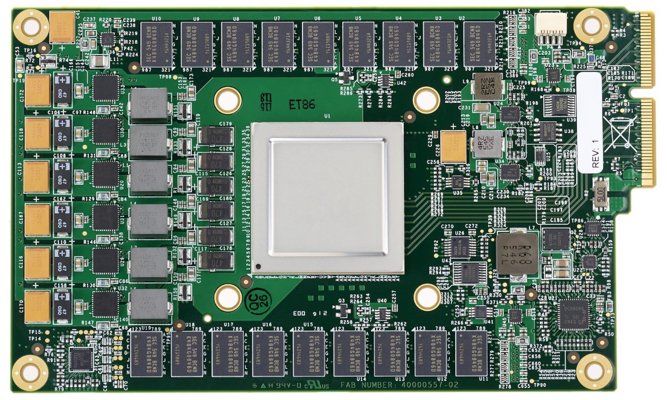
Fig 3. TPU Printed Circuit Board. It can be inserted in the slot for an SATA disk in a server, but the card uses PCIe Gen3 x16.
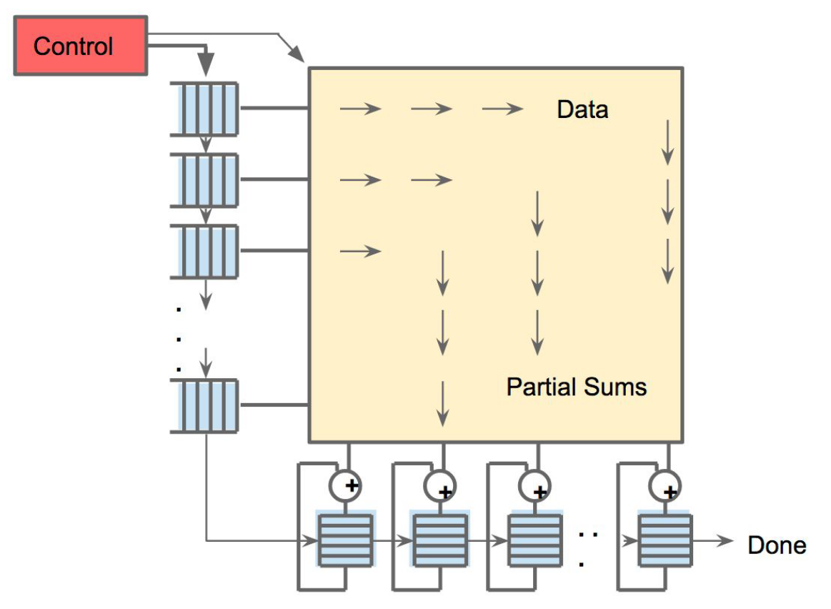
Fig 4. Systolic data flow of the Matrix Multiply Unit. Software has the illusion that each 256B input is read at once, and they instantly update one location of each of 256 accumulator RAMs.
Understanding More
To understand why TPUs were designed the way they were, consider the calculations involved in running a simple neural network.
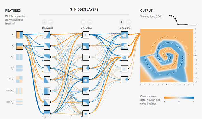
Fig 5. Double spiral problem on TensorFlow Playground (click here to try it)
This example trains a neural network to classify a data point as blue or orange. The process of running a trained neural network to classify data or estimate values is called inference. For inference, each neuron does:
- Multiply the input data (x) with weights (w) to represent signal strength
- Add the results to aggregate the neuron's state into a single value
- Apply an activation function (f) to modulate the artificial neuron's activity
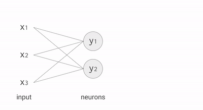
Even for a simple single-layer fully-connected network with three inputs and two neurons, you need six multiplications and two groups of additions — a sequence that can be written as a matrix multiplication. Matrix multiplications are often the most computationally intensive part of inference.
The number of weights per network varies enormously across production models:
| Type of network | # of layers | # of weights | % of deployed |
|---|---|---|---|
| MLP0 | 5 | 20M | 61% |
| MLP1 | 4 | 5M | — |
| LSTM0 | 58 | 52M | 29% |
| LSTM1 | 56 | 34M | — |
| CNN0 | 16 | 8M | 5% |
| CNN1 | 89 | 100M | — |
Every prediction requires many steps of multiplying processed inputs by a weight matrix and applying an activation function. To reduce resource requirements, a technique called quantization lets us work with integer operations rather than 32-bit or 16-bit floating point, reducing total memory and compute needed.
Parallel Processing on the Matrix Multiplier Unit
Typical RISC processors are scalar processors — they process a single operation per instruction. Even at gigahertz clock speeds, large matrix operations via scalar instructions can be slow. Vector processing improves this by performing the same operation across many data elements concurrently. CPUs incorporate extensions like SSE and AVX; GPU streaming multiprocessors (SMs) are effectively vector processors with thousands of ALUs on a single die.
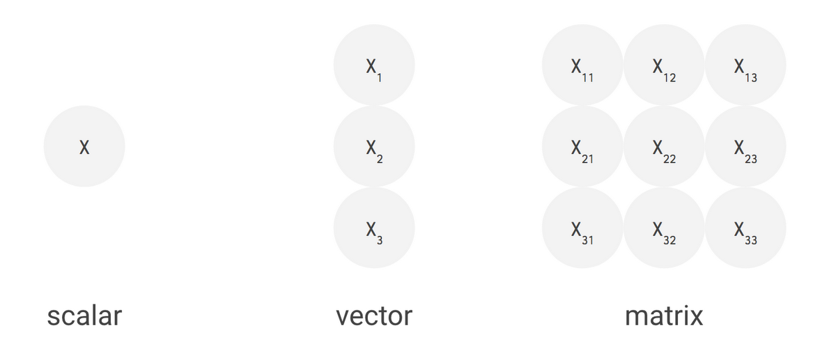
Fig 6. Scalar, vector and matrix processing.
The TPU's MXU is a matrix processor that processes hundreds of thousands of operations in a single clock cycle — analogous to printing one character at a time, one line at a time, or an entire page at a time.
The Heart of the TPU: A Systolic Array
The MXU uses a systolic array — a drastically different architecture from typical CPUs and GPUs. CPUs are general-purpose: they store values in registers and use programmed control to direct ALUs. All of these features (registers, ALUs, programmed control) cost power and chip area.
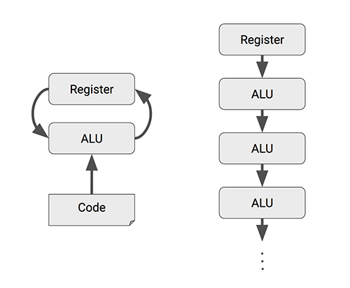
Fig 7. CPUs and GPUs often spend energy to access multiple registers per operation. A systolic array chains multiple ALUs together, reusing the result of reading a single register.
For matrix multiplication, each input value is reused many times. In the MXU, wires only connect spatially adjacent ALUs (short and energy-efficient), and ALUs perform only multiplications and additions in fixed patterns. Data flows through the chip in waves — reminiscent of the heart pumping blood — hence "systolic."
The TPU Matrix Multiplication Unit has a systolic array with 256 × 256 = 65,536 ALUs. Running at 700 MHz, it can compute 65,536 × 700,000,000 = 46 × 10¹² multiply-and-add operations per second, or 92 Teraops/s in the matrix unit.
| Processor | Operations per cycle |
|---|---|
| CPU | a few |
| CPU (vector extension) | tens |
| GPU | tens of thousands |
| TPU | hundreds of thousands, up to 128K |
During the massive matrix multiply, all intermediate results pass directly between 64K ALUs without any memory access, significantly reducing power consumption and increasing throughput. The result: TPU provides an 83× better performance-per-watt ratio compared with contemporary CPUs and 29× better than contemporary GPUs.
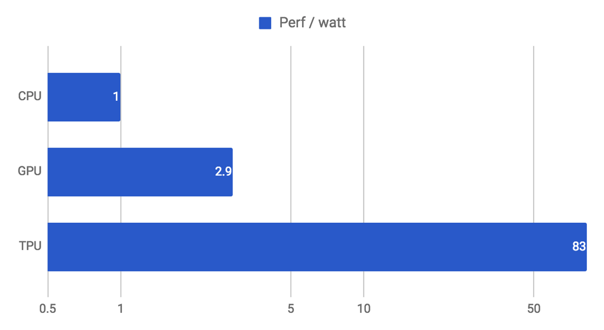
Fig 8. Performance / watt, relative to contemporary CPUs and GPUs (log scale, incremental weighted mean).
Instruction Set
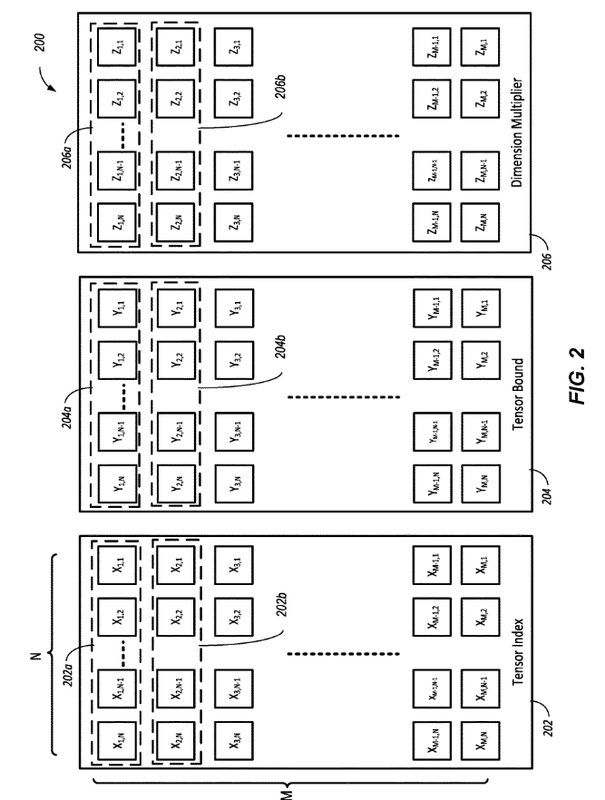
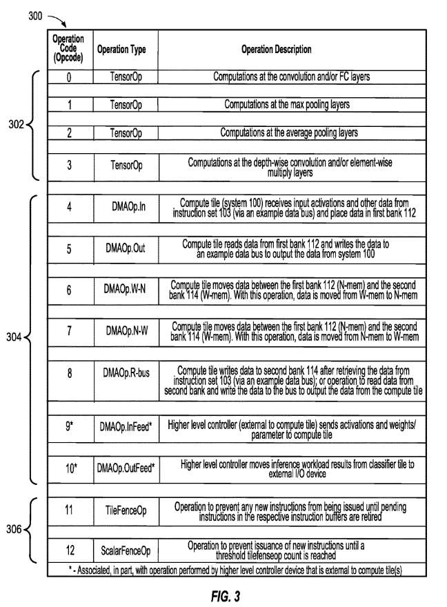
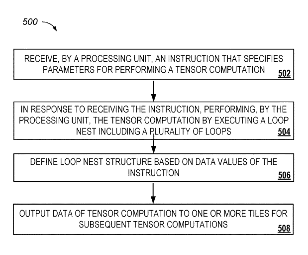
A TPU receives instructions that specify data values for performing a tensor computation. In response, the TPU performs the computation by executing a loop nest whose structure is defined by values in the instruction. The tensor computation is typically at least a portion of a neural network layer computation. The instruction values may include a value specifying the type of the neural network layer, which also determines the loop nest structure.
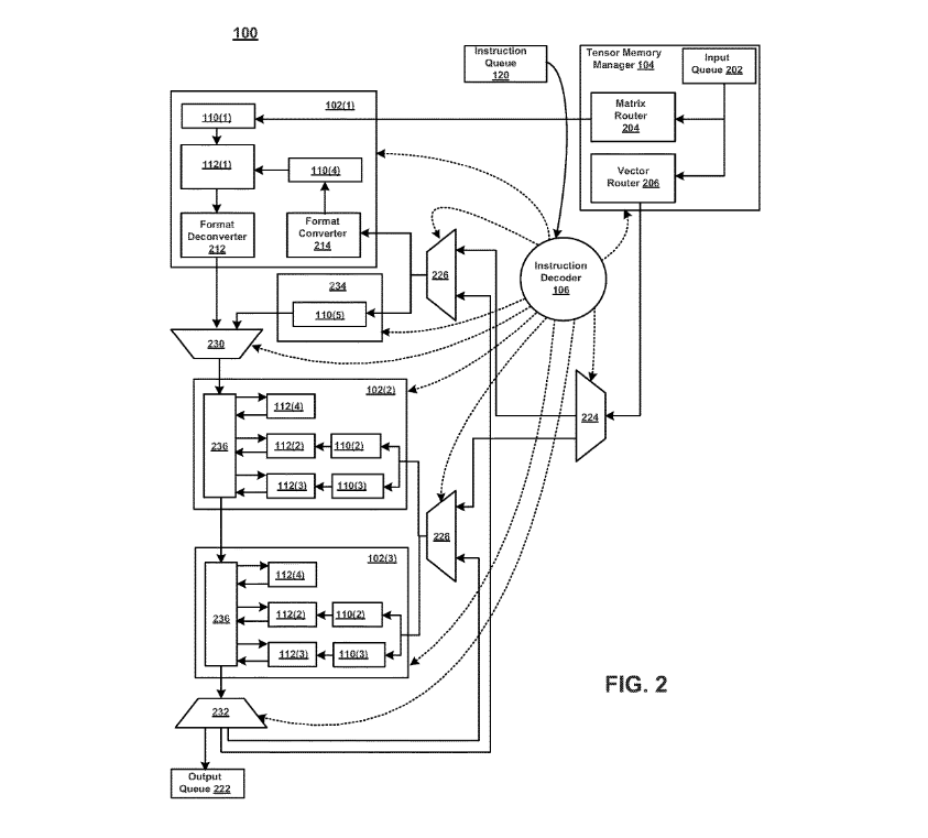
Flow Diagram
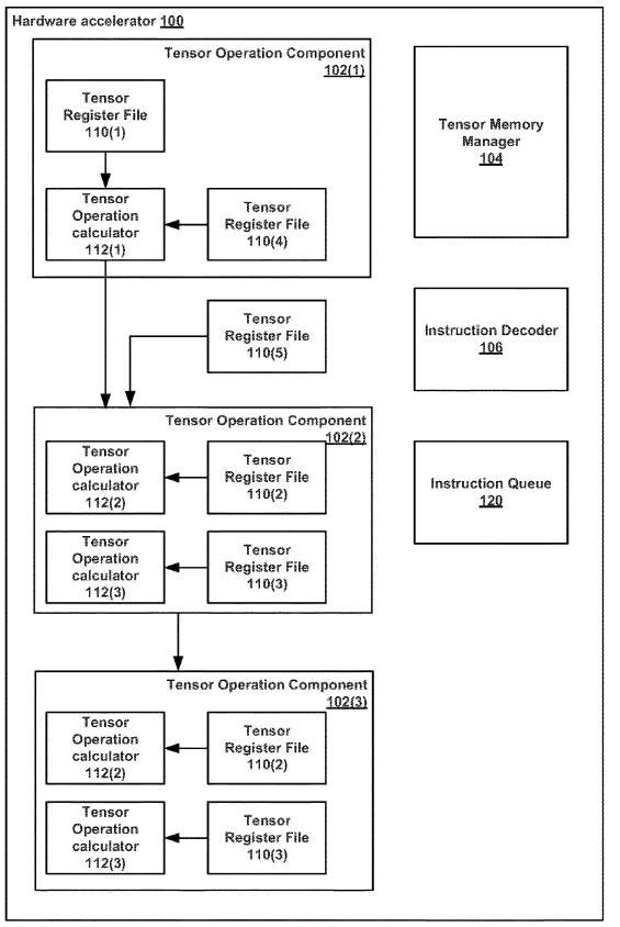
A hardware accelerator with an efficient instruction set is disclosed. An apparatus may comprise logic configured to access a first and a second machine instruction. The second machine instruction may be missing a tensor operand needed for its execution. The logic may be further configured to execute the first machine instruction, producing a tensor, and then execute the second machine instruction using that resultant tensor as the missing tensor operand.
Conclusion
The TPU succeeded because of the large — but not too large — matrix multiply unit; the substantial software-controlled on-chip memory; the ability to run whole inference models to reduce dependence on the host CPU; a single-threaded, deterministic execution model that proved to be a good match to 99th-percentile response time limits; enough flexibility to match the NNs of 2017 as well as of 2013; the omission of general-purpose features that enabled a small and low-power die despite the larger data path and memory; the use of 8-bit integers by quantized applications; and that applications were written using TensorFlow, which made them easy to port to the TPU at high performance rather than requiring a complete rewrite. Order-of-magnitude differences between commercial products are rare in computer architecture, which may lead the TPU to become an archetype for domain-specific architectures.
Works Cited
Norman P. Jouppi, Cliff Young, Nishant Patil. In-Datacenter Performance Analysis of a Tensor Processing Unit, 2017.
https://patentimages.storage.googleapis.com/78/54/ba/c1e8901029486c/US20180341484A1.pdf
https://patentimages.storage.googleapis.com/11/74/c4/8390c55ced8356/US9836691.pdf
Abadi, M., Agarwal, A., Barham, P., Brevdo, E., Chen, Z., Citro, C., Corrado, G.S., Davis, A., Dean, J., Devin, M. and Ghemawat, S., 2016. TensorFlow: Large-scale machine learning on heterogeneous distributed systems. arXiv preprint arXiv:1603.04467.
Jouppi, N. May 18, 2016. Google supercharges machine learning tasks with TPU custom chip. https://cloudplatform.googleblog.com
Hennessy, J.L. and Patterson, D.A., 2018. Computer Architecture: A Quantitative Approach, 6th edition, Elsevier.
Shivaram. https://pages.cs.wisc.edu/~shivaram/cs744-fa21-slides/cs744-tpu-notes.pdf
https://www.kaggle.com/docs/tpu
https://cloud.google.com/tpu/docs/system-architecture-tpu-vm
https://www.tomshardware.com/news/google-tensor-processing-unit-machine-learning,31834.html
Cite This Post
Auto-generated. Verify for your institution's requirements.